


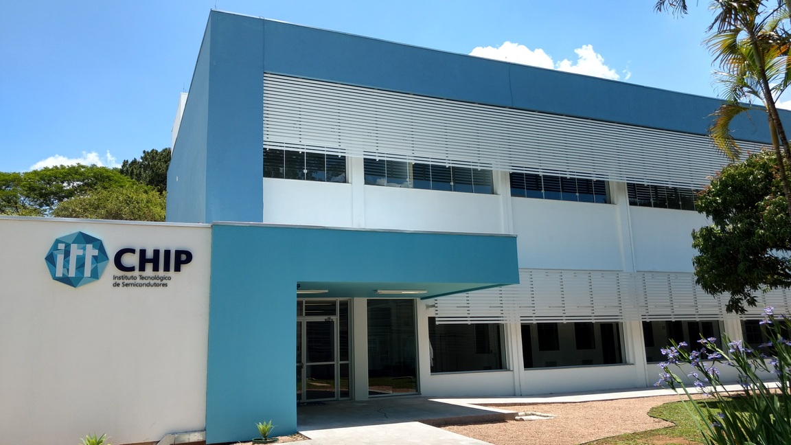
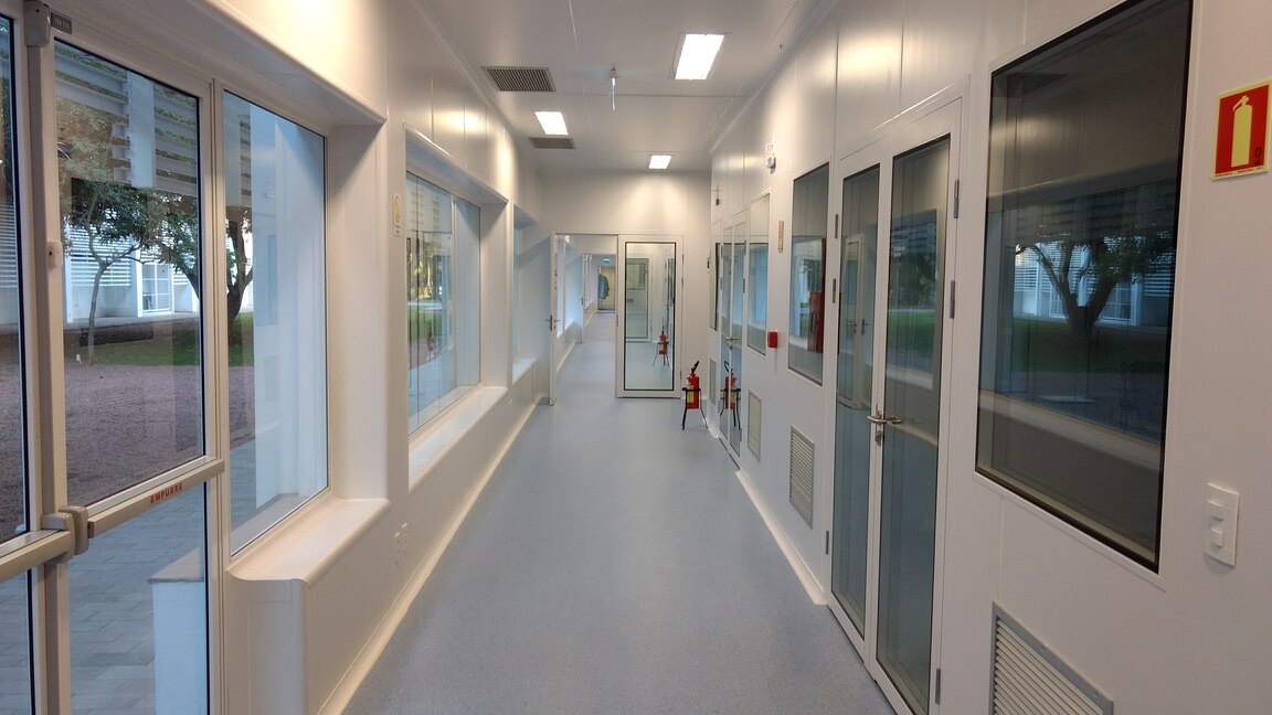
Infrastructure and Laboratories
Research and technological solutions for companies focused on the development of products and projects for chip packaging, multicomponent (SiP), IoT solutions, microdevices and sensors.
Infrastructure
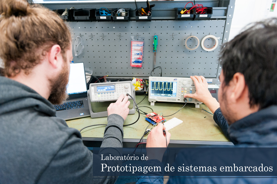
The institute has a series of laboratories in a total area of 2,500 m2, with 750 m2 of clean rooms that are environments with humidity, temperature and particle concentration controlled in 3 cleaning classes, class 100,000 (ISO-8), class 10,000 (ISO-7) and class 1000 (ISO-6). It is the largest university clean room in Latin America. Also available are electromechanical facilities such as dry and oil-free compressed air, nitrogen, heat and chemical vapor exhaust, single-phase and three-phase electric power, common and deionized water and drains. There are also rooms for training, rooms for researchers and students.
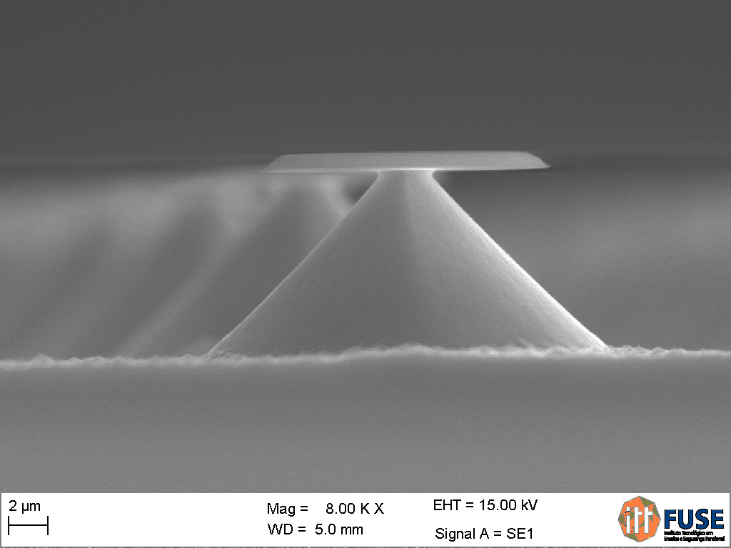
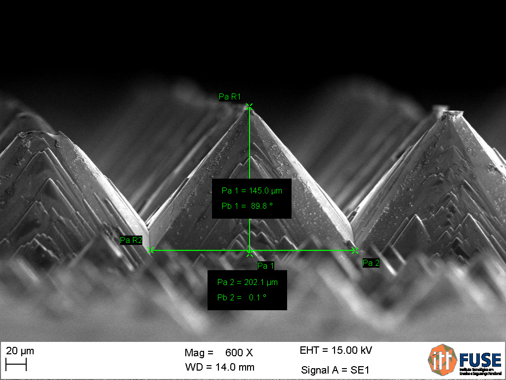
Laboratories
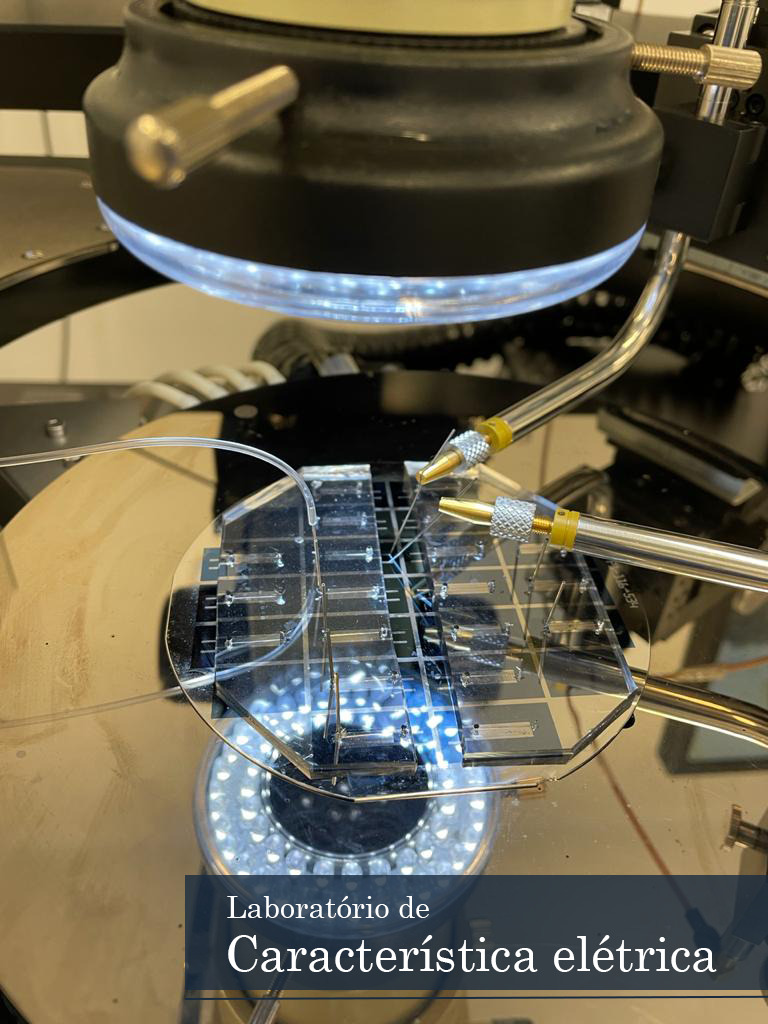
specialized in the design of multi-component integrated circuits, mainly SiP – System in Package type, for IoT applications. It has a complete set of Cadence design tools plus Ansys, Comsol and Labview simulation tools for testing. Also, it has a set of digital, analog and RF test and characterization tools, in addition to having the entire prototyping infrastructure of the itt Chip (SMT and Packaging Laboratories). It has a multidisciplinary team of designers and specialists, around 12, in packaging, RF, firmware, digital design and testing. The Design Center works in direct partnership with HT Micron Semiconductors, allowing the products (mainly SiPs) developed to be produced in volume at the HT Micron factory. After design validation, the products can be transferred to immediate production at HT.
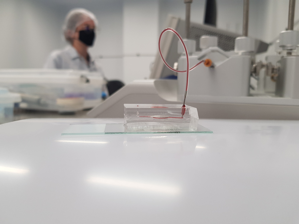
The Flexible Electronics Laboratory has equipment for the preparation and characterization of various materials, mainly for flexible electronics applications such as conductive inks based on nanomaterials, semiconductor polymers and conductive adhesives. It has a high resolution ink-jet printer (Dimatix DMP 2831), four-point resistivity meter (Signatone Pro4-4000), high-speed centrifuge (Hitachi CF15RN), profilometer (KLA-TENCOR D-500 ), galvanostat potentiostat (Autolab PG-302N), oven (ETHIK 400-3ND), ultrasonic bath (ALPAX LSUC2-120-3.0, 40Hz 120W) , pH meter (TECNAL TEC-5), magnetic stirrer with heating (Tecnal TE-0851), vortex mixer (Kasvi), analytical and semi analytical balance (Sartorius and Shimatdzu) and chemical hood (Produlab).
Contact us
Our team is ready to offer technological support to your company and enhance your business development capacity.
Address
Semiconductor Technology Institute - itt Chip
Av. Unisinos, 950 – São Leopoldo - RS / Building F04 - Access by Gate 4 / Sector F
Av. Unisinos, 950 – São Leopoldo - RS / Building F04 - Access by Gate 4 / Sector F
Phone
+55 (51) 3590-8483 - Extension number: 3180 or 3183